

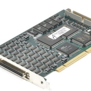
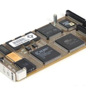
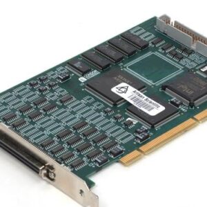
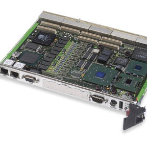
The Agilent/Keysight 4083A is a DC/RF parametric test system engineered for high-volume semiconductor manufacturing. It performs automated on-wafer testing, combining DC and RF S-parameter measurements to address the demands of advanced process nodes with shrinking lithographies and emerging device technologies.
– Technical Specifications
• RF ports: 10
• DC pins: up to 48
• Direct-docking probe card interface with operator or automated probe card changer support
• Optional RF matrix for measurement of up to 5 RF test structures in single touchdown
• Integrated PNA option supports S-parameter and RFCV measurements
• Automated RF calibration routines including SOLT, SOL, and Open/Short de-embedding
• Test data storage in ADT format with raw measurements, statistical data (average, standard deviation), and bin/yield information
– Key Features
• On-wafer S-parameter measurement capability in production environment
• Integration with Agilent/Keysight PNA series vector network analyzers
• Reduced RF probe card wear through multi-structure measurement per touchdown
• Automated calibration routines operable by technicians or operators
• Support for high-k gate dielectrics, strained silicon, flash memory cells, and high-speed processes
– Typical Applications
• Parametric characterization of advanced semiconductor devices
• Production test of RF and mixed-signal components
• High-volume on-wafer device evaluation
• Automated yield monitoring in lights-out environments
– Compatibility & Integration
• SPECS (Semiconductor Process Evaluation Core Software) compatible
• SPECS-FA software support with SEMI standards compliance for automated production monitoring
• Test plans and algorithms from 4070 Series platforms run without modification on Linux-based 4080 Series platforms
• Direct integration with Agilent/Keysight PNA measurement instruments


Reviews
There are no reviews yet.