


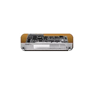
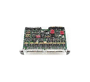
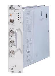
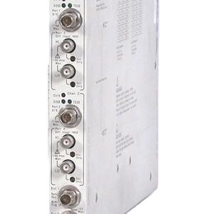
The Agilent/Keysight J1421A is a clock source module for high-speed digital testing within VXI instrumentation systems. It generates precise clock signals at 10 Gb/s and 2.5 Gb/s, with clock offset capability of ±20 ppm. The module accepts multiple external reference sources—156 MHz, 622 MHz, and 2.5 GHz—and external clock inputs at 10 GHz and 2.5 GHz. It can slave to a 156 MHz clock recovered from a J1420B Receiver module, making it essential for network analysis and bit error rate testing applications requiring stable, synchronized timing signals.
– Technical Specifications
• Product Type: Clock Source VXI Module
• Form Factor: C-size, two-slot VXI module
• Register-Based: Yes
• Clock Generation: 10 Gb/s and 2.5 Gb/s outputs
• Clock Offset: ±20 ppm
• External Reference Source Input: 156 MHz, 622 MHz, 2.5 GHz
• External Clock Input: 10 GHz, 2.5 GHz
• Slaving Capability: 156 MHz recovered clock from J1420B Receiver module
– Key Features
• Dual clock generation at industry-standard data rates for high-speed testing
• Multiple reference input options for flexible system synchronization
• Fine clock offset tuning for precision measurements
• Direct integration with Agilent/Keysight receiver modules via slaving capability
• Part of the SpectralBER Clock Source product family
– Typical Applications
• Bit Error Rate (BERT) testing on high-speed digital signals
• Network analyzer clock sourcing
• Synchronization within VXI-based instrumentation systems
– Compatibility & Integration
The J1421A integrates into standard VXI chassis and works with the J1420B Receiver module for clock recovery and synchronization. Its register-based architecture enables straightforward control and configuration within larger test systems.


Reviews
There are no reviews yet.