

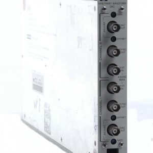
The NI PCI-5421 is a 16-bit arbitrary waveform generator with LVDS digital outputs, delivering precise analog and digital signal generation for demanding test applications. It combines a 100 MS/s native sample rate with up to 400 MS/s effective sampling via interpolation, Direct Digital Synthesis (DDS) architecture, and the Synchronization and Memory Core (SMC) for flexible waveform and instruction parameterization. The device generates user-defined arbitrary waveforms and standard functions—sine, square, triangle, and ramp—with output levels spanning -6 V to +6 V (12 Vp-p into 50 Ω). Onboard memory scales from 8 MB to 512 MB to accommodate complex signal sequences. The analog channel delivers 91 dBc close-in SFDR, -62 dBc THD at 10 MHz, and sub-1.0 psrms jitter. Optional 16-bit LVDS digital pattern output provides direct access to the waveform digital representation, synchronized to the sample clock. Two bidirectional SMB channels support trigger inputs (DC to 105 MHz) or event generator outputs, enabling flexible system integration. A 43 MHz 7-pole elliptical filter suppresses high-frequency images, while software-selectable output impedance (50 Ω or 75 Ω) and variable attenuation optimize signal conditioning. The direct-path bypass mode delivers ±0.25 dB passband flatness from 0 to 40 MHz for IF applications. Output summing from multiple modules simplifies multi-channel signal synthesis.
– Technical Specifications
• 16-bit DAC resolution with -6 V to +6 V output range (12 Vp-p into 50 Ω)
• 100 MS/s native sample rate; 400 MS/s effective with 2x, 4x, or 8x interpolation
• 91 dBc close-in spurious-free dynamic range
• -62 dBc total harmonic distortion at 10 MHz
• -148 dBm/Hz average noise density
• <1.0 psrms jitter at analog output
• <5% pulse aberration
• 43 MHz 7-pole elliptical analog filter
• Onboard memory: 8 MB, 32 MB, 256 MB, or 512 MB configurations
• 16-bit LVDS digital pattern output with DDC CLK OUT synchronization
• Software-selectable output impedance: 50 Ω or 75 Ω
• ±0.25 dB passband flatness (0 to 40 MHz) via direct bypass path
– Key Features
• Direct Digital Synthesis for accurate waveform generation
• Arbitrary waveform and standard function generation (sine, square, triangle, ramp)
• Synchronization and Memory Core (SMC) architecture for shared waveform/instruction memory
• Variable output attenuation with three-digit precision
• LVDS digital outputs showing real-time 16-bit waveform representation
• Two bidirectional trigger channels: DC to 105 MHz input range, -2 V to +7 V max overload
• VHDCI 68-pin connector with LVDS pattern output and programmable control signals
• Waveform summing support across multiple modules
– Typical Applications
• Communications signal generation and testing
• Aerospace and defense system validation
• Semiconductor device characterization
• IF signal synthesis and modulation
– Compatibility & Integration
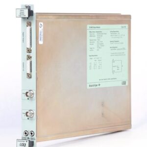
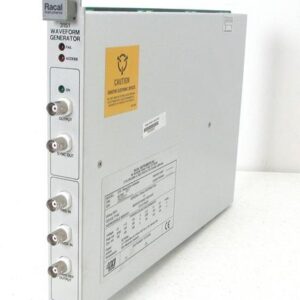
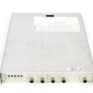
PCI form factor. One SMB analog output, two SMB bidirectional channels, optional 68-pin VHDCI DDC connector.


Reviews
There are no reviews yet.