

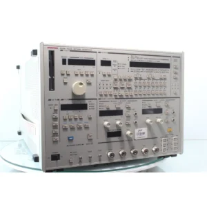
The Tektronix HFS9009 Stimulus System is a modular, high-performance signal generation platform for precise electronic device characterization. It combines data generation, pulse generation, and switch matrix functionality in a fully digital architecture, delivering picosecond-level timing resolution and flexible multi-channel output configurations. Paired with a high-speed digitizing oscilloscope, the system enables comprehensive testing with up to 36 channels per mainframe, phase-locked operation, and advanced timing alignment capabilities.
– Technical Specifications
Time Base Performance
• Frequency range: 50 kHz to 630 MHz
• Frequency resolution: <0.1% of programmed value
• Frequency accuracy: ±1% of programmed value
• RMS jitter: 15 ps ±0.05% of interval
• Phase lock-in frequency range: 6 MHz to 630 MHz
• Phase lock-in amplitude range: 0.8 V to 1.0 V peak-to-peak
• Output frequency: Any 2n multiple or submultiple of phase lock-in frequency, within installed card range
• Frame sync input: Initiates burst with external frequency reference
Output Edge Placement
• Channel deskew range: -60 ns to 2.0 µs
• Channel deskew resolution: 1 ps
• Delay adjust range: 0 to 20 µs
• Delay adjust resolution: 1 ps
• Delay accuracy: 1% ±50 ps
• Width adjust range: 0 to 65,536 periods
• Width adjust resolution: 1 ps
Output Performance
• Level resolution: 0.01 V
• HIGH level accuracy: ±2% of level ±50 mV
• LOW level accuracy: ±2% of HIGH level ±2% of amplitude ±50 mV
• Output aberrations (200 ps after 50% point): Overshoot +15% +20 mV, undershoot -10% -20 mV
• Maximum HIGH level: +5.00 V (HFS9DG1), +5.50 V (HFS9DG2)
• Minimum LOW level: -2.50 V (HFS9DG1), -2.00 V (HFS9DG2)
• Peak-to-peak amplitude range: 10 mV to 3.00 V (HFS9DG1), 10 mV to 5.50 V (HFS9DG2)
• Output transition time: <250 ps (<1 V p-p), 800 ps to 6 ns (variable)
Trigger Input
• Input impedance: 50 Ω
• Input voltage range: ±5 V maximum
• Programmable threshold range: -4.70 V to +4.70 V
• Programmable threshold resolution: 100 mV
• Programmable threshold accuracy: ±100 mV ±5% of level
• Minimum input pulse width: 1 ns
• Input rise/fall time requirement: <10 ns
• Sensitivity: <500 mV
Power
• Line voltage: 90 V AC to 130 V AC RMS, or 180 V AC to 250 V AC RMS (auto-switched)
– Key Features
• Fully digital architecture enables flexible pulse edge placement
• Picosecond timing resolution (1 ps) across delay and width adjustment
• Phase-locked multi-channel operation with programmable output frequency
• Channel deskew with -60 ns to 2.0 µs range supports timing synchronization
• HFS9DG1 and HFS9DG2 card options for output voltage and accuracy optimization
• Modular mainframe design scales to 36 channels
• Frame sync triggering from external sources
– Typical Applications
• High-speed digital device testing and validation
• Timing characterization of integrated circuits and subsystems
• Multi-channel stimulus generation with precise phase alignment
• Edge placement and rise/fall time parameter measurement
– Compatibility & Integration
The HFS9009 integrates with high-speed digitizing oscilloscopes to form complete measurement systems. Phase lock-in capability supports external frequency references, enabling synchronization with external test environments. Modular card architecture accommodates both HFS9DG1 and HFS9DG2 output stages within a single mainframe.


Reviews
There are no reviews yet.